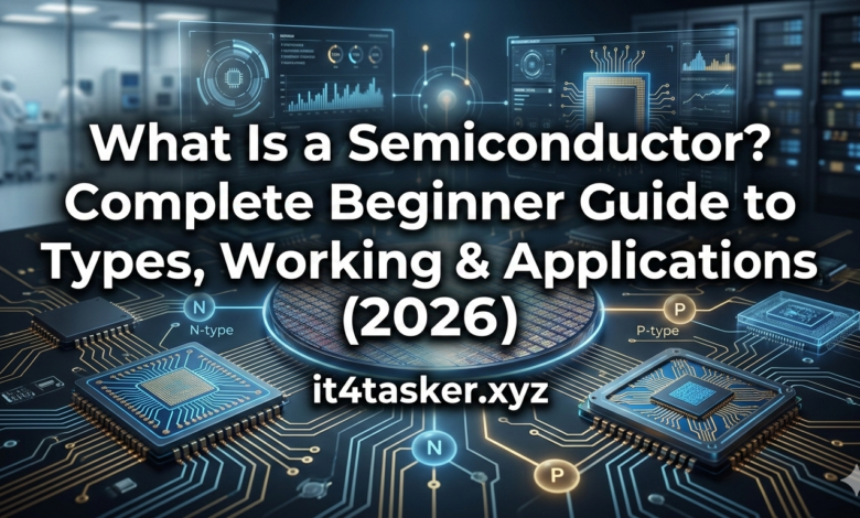
What Is a Semiconductor? Complete Beginner Guide to Types, Working & Applications (2026):
Introduction:
The digital world depends on Semiconductors for everything from phones to smart tools. They act as a bridge between conductors and insulators in Modern Electronics. Every big industry needs them to grow.
Looking ahead to 2026 Technology Trends, we see a need for smaller, faster parts. Engineers are working hard to make efficient hardware for the future. This effort is making smart systems more common worldwide.

It’s crucial to understand the roles of these parts for industry leaders. This guide helps us see the fast world of high-speed computing. We’ll explore how these materials will shape the next decade.
New techniques allow for unmatched precision at the atomic level. This ensures future devices will be powerful. It’s important for professionals to stay updated to stay ahead in the market.
Key Takeaways
- Understanding current chip roles in global tech.
- Future shifts in hardware manufacturing.
- How conductivity levels impact device performance.
- Growth of smart systems in various industries.
- Importance of energy-efficient design for new tools.
- Navigating the high-speed computing landscape.
What Is a Semiconductor? Types, Working Principle & Applications (2026 Guide)
Understanding semiconductors is key to grasping modern electronics. They are the heart of the electronics world. They make devices smaller, faster, and more efficient.
Defining Semiconductors in Modern Electronics
Semiconductors are materials that are not as good at conducting electricity as metals but better than insulators. This special ability lets them control electrical current flow. Types of semiconductors include intrinsic and extrinsic, each with its own uses.
The working principle of semiconductors is their ability to be “doped” with impurities. This changes their electrical properties. It helps make different semiconductor devices.

Why Semiconductors Matter in 2026
In 2026, semiconductors will still be crucial for technology progress. They are used in computing, telecommunications, automotive electronics, and renewable energy systems.
The need for semiconductors grows as we want faster, more efficient devices. As technology advances, semiconductors will become even more important. This will drive innovation and growth in the industry.
The Fundamental Physics Behind Semiconductors
The physics of semiconductors is quite interesting. It involves the atomic structure, how electrons behave, and energy band theory.
Atomic Structure and Electron Behavior
Semiconductors are usually made from silicon or germanium. These elements have four valence electrons. These electrons bond with other atoms, forming a crystal lattice.
The way electrons move in this lattice is key to understanding semiconductors. The arrangement of electrons and their bonds affect the material’s electrical properties.
Energy Band Theory Explained
The energy band theory is crucial for semiconductors. In solids, the energy levels of atoms merge into bands.
The valence band is full of electrons, while the conduction band is empty. The gap between these bands, called the bandgap, decides how well the material conducts electricity.
Conductivity Between Insulators and Conductors
Semiconductors have a conductivity level between insulators and conductors. This is because their bandgap is smaller than insulators but larger than conductors.
At absolute zero, semiconductors act like insulators. But as temperature rises, electrons get enough energy to cross the bandgap. This lets them conduct electricity.

| Material Type | Bandgap | Conductivity |
|---|---|---|
| Insulators | Large | Low |
| Semiconductors | Moderate | Moderate |
| Conductors | Small or Overlapping Bands | High |
The physics behind semiconductors is complex and fascinating. It’s the foundation of modern electronics.
Understanding atomic structure, electron behavior, and energy band theory helps us see how semiconductors work. This unique conductivity is what makes them so important.
Intrinsic Semiconductors: Pure Silicon and Germanium
Pure silicon and germanium are key to intrinsic semiconductors. They show us the basics of how semiconductors work. These materials are pure, without any impurities.
Crystal Lattice Structure
These semiconductors have a special structure called a crystal lattice. Each atom is connected to its neighbors in a repeating pattern. This pattern is crucial for their electrical properties.
For example, silicon atoms are bonded to four neighbors, forming a tetrahedral shape. This shape is important for understanding how these semiconductors conduct electricity.
The lattice is not perfect and can change with temperature. At absolute zero, it’s perfect, and the material is an insulator. But as temperature rises, thermal energy excites electrons, allowing them to move and conduct.
Temperature Effects on Intrinsic Semiconductors
Temperature greatly affects how well intrinsic semiconductors conduct. As temperature goes up, more electrons get enough energy to move from the valence band to the conduction band. This increases the number of charge carriers, making the material more conductive.
The relationship between temperature and conductivity is exponential. This means small temperature increases can greatly improve conductivity. But it also makes these semiconductors very sensitive to temperature changes.
In summary, intrinsic semiconductors from pure silicon and germanium are essential for understanding semiconductor technology. Their crystal lattice and how temperature affects their conductivity are key to their use in many electronic devices.
Extrinsic Semiconductors and the Doping Process
Extrinsic semiconductors are made by adding impurities to intrinsic semiconductors. This changes their electrical properties. It’s key for making semiconductors for different uses.
What Is Doping and Why It Matters
Doping means adding impurities to the crystal lattice of intrinsic semiconductors. These impurities can add extra electrons or holes. This changes how well the semiconductor conducts electricity.
The type of dopant used depends on what electrical properties are needed. This is why doping is so important. It lets manufacturers make semiconductors with specific properties.
Donor and Acceptor Impurities
Donor impurities have more valence electrons than the semiconductor. For example, phosphorus has five valence electrons when added to silicon. This extra electron can move freely, making the semiconductor more conductive.
Acceptor impurities have fewer valence electrons. Boron, with three valence electrons, is used in silicon as an acceptor. It creates holes that can accept electrons, increasing the semiconductor’s hole concentration.
Controlling Electrical Properties
By changing the type and amount of dopants, semiconductors’ electrical properties can be controlled. This is crucial for making devices like diodes and transistors.
Doping has been key in making modern electronics. It helps create complex components for many technologies. These include computers, phones, and medical devices.
N-Type Semiconductors: Electron-Rich Materials
N-Type semiconductors are key in today’s electronics. They are made by adding special impurities to silicon. This changes how they conduct electricity.
Phosphorus and Arsenic as Dopants
Phosphorus and arsenic are top choices for doping. They have five valence electrons, which means they can share four and still have one to donate. This makes the semiconductor more conductive.
Phosphorus and arsenic are great for several reasons:
- They dissolve well in silicon
- They easily give away electrons
- They work well at different temperatures
Majority and Minority Carriers in N-Type
N-Type semiconductors have lots of free electrons. These electrons are the main charge carriers.
These majority carriers affect how well N-Type semiconductors conduct electricity. But, we also need to talk about minority carriers. In N-Type semiconductors, these are holes.
| Carrier Type | Description | Concentration |
|---|---|---|
| Majority Carriers | Electrons | High |
| Minority Carriers | Holes | Low |
Experts say, “Knowing the difference between majority and minority carriers is key to understanding semiconductors.”
P-Type Semiconductors: Hole-Dominated Materials
P-Type materials are made by adding special impurities to pure semiconductors. They are key for many electronic devices. These materials are created by adding acceptor impurities, usually from Group III, to the semiconductors.
Boron and Gallium Doping
Doping is vital in making P-Type semiconductors. Boron and Gallium are common dopants. They have fewer valence electrons than the semiconductor, like Silicon.
By adding Boron or Gallium to Silicon, they replace Silicon atoms. Since they have fewer electrons, they create “holes.” This makes the material P-Type.
Understanding Hole Movement
In P-Type semiconductors, hole movement is key. Holes are not actual particles but the lack of electrons. When an electric field is applied, holes move like positive charges.
Holes move by electron transfer between atoms. When an electron fills a hole, it creates another hole. This makes it seem like the hole is moving. This process is vital for many semiconductor devices.
Knowing how P-Type semiconductors and holes work is essential. It helps in making many electronic parts, from simple diodes to complex circuits.
Semiconductor Materials Used in Modern Electronics
The world of semiconductors is always changing. New materials are being found to make electronics better and more efficient. The material used is key because it affects how well and how much something costs.
Silicon: The Industry Standard
Silicon is the top choice for semiconductors. It’s common, well-studied, and easy to make. Silicon’s dominance comes from its perfect bandgap, fitting for many uses, from gadgets to industrial tools.
The silicon industry has a strong supply chain. This has lowered costs and made silicon products very competitive.
Gallium Arsenide for High-Speed Applications
Gallium Arsenide (GaAs) is key for fast and high-frequency needs. GaAs has better electron mobility than silicon. It’s great for microwave and optoelectronic devices, and fast circuits.
GaAs is used in satellites, radar, and some wireless devices. But, it’s pricier and rarer than silicon, which limits its use.
Silicon Carbide and Gallium Nitride for Power Electronics
Silicon Carbide (SiC) and Gallium Nitride (GaN) are new stars in power electronics. SiC and GaN have better properties than silicon, like higher voltage and speed, and better heat handling.
They’re used in electric cars, green energy, and heavy-duty industries. Their high performance is perfect for tough jobs.
Emerging Materials: Graphene and 2D Semiconductors
Graphene and 2D semiconductors are the future. Graphene’s amazing electrical and mechanical abilities make it great for thin, flexible, and efficient electronics.
Work on 2D semiconductors is ongoing. Challenges like making them bigger, integrating them, and manufacturing are being tackled. Their uses could be huge, from bendy electronics to super-fast transistors.
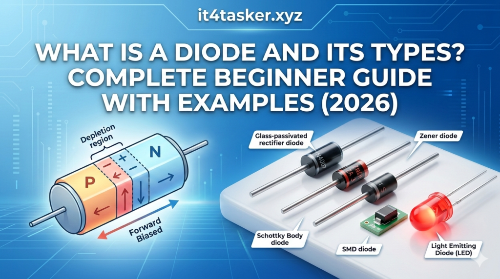
How Semiconductors Work: The PN Junction
The PN junction is at the core of how semiconductors work. It’s formed by combining P-type and N-type materials. This junction is key to understanding how semiconductors manage electrical current.
Formation of the Depletion Region
The PN junction is made by adding different impurities to a semiconductor. This creates P-type and N-type regions. When these regions meet, electrons from the N-type move into the P-type, and holes from the P-type move into the N-type.
This movement creates a depletion region around the junction. This area lacks charge carriers. The depletion region acts as a barrier, opposing the movement of charge carriers across the junction.
Forward and Reverse Bias Conditions
The PN junction’s behavior changes with bias conditions. A positive voltage on the P-type and a negative on the N-type makes it forward-biased. This narrows the depletion region, allowing current to flow.
On the other hand, a negative voltage on the P-type and a positive on the N-type makes it reverse-biased. This widens the depletion region, stopping current flow.
Current Flow Mechanisms
Under forward bias, the junction’s reduced depletion region lets majority carriers cross. This results in current flow. In contrast, reverse bias widens the depletion region, stopping majority carriers from crossing and reducing current flow.
Table: PN Junction Behavior Under Different Bias Conditions
| Bias Condition | Depletion Region Width | Current Flow |
|---|---|---|
| Forward Bias | Decreases | Increases |
| Reverse Bias | Increases | Decreases |
Essential Semiconductor Devices and Components
Modern electronics rely on semiconductor devices. They control electrical current flow. This is key for everything from simple circuits to complex computers.
Diodes: One-Way Current Flow
Diodes let current flow in one direction but block it in the other. This is why they’re vital for turning AC to DC. Diodes also help with voltage control and signal changes, important in power supplies and communication.
Transistors: The Building Blocks of Modern Electronics
Transistors are crucial for electronics, acting as amplifiers or switches. They’re the foundation of modern electronics. The invention of the transistor changed electronics, making devices smaller and more efficient.
Integrated Circuits and Microchips
Integrated circuits (ICs) put many devices on one chip, usually silicon. This led to microprocessors and memory chips. ICs have made devices smaller, more powerful, and cheaper.
MOSFETs and Power Semiconductor Devices
MOSFETs are used for signal amplification or switching. They’re great for digital circuits because they use little power. Power devices like MOSFETs and IGBTs handle big voltages and currents. They’re key for controlling motors and in renewable energy systems.
Semiconductor Manufacturing Processes in 2026
The year 2026 has seen big steps forward in semiconductor manufacturing. These steps are making processes more advanced to meet today’s electronics needs.
Technology keeps getting better, and so do the ways we make semiconductors. We’re using new materials and methods to keep semiconductors at the center of new ideas.
Wafer Fabrication and Photolithography
Wafer fabrication is key in making semiconductors. It’s where we create the silicon wafer for electronic circuits.
Photolithography plays a big role in this. It uses light to draw patterns on the semiconductor material. This method has improved a lot, making it possible to create smaller, more detailed circuits.
Experts say, “Photolithography’s need for precision has led to extreme ultraviolet lithography (EUVL). It’s now used in top-notch fabs.”
Advanced Node Technology: 3nm and Beyond
The push for advanced node technology keeps going, aiming for 3nm and beyond.
These steps help make chips more powerful and efficient. They’re key for advancements in artificial intelligence, 5G, and the Internet of Things (IoT).
- Improved performance and power efficiency
- Increased transistor density
- Enhanced functionality
Quality Control and Testing Procedures
Quality is crucial in semiconductor devices. That’s why there are strict testing procedures to find any defects or problems.
Quality control uses many methods, from simple checks to complex electrical tests.
As technology advances, so does the need for strong quality control. It’s vital for the reliability and performance of the final product.
Applications of Semiconductors in Modern Electronics
Semiconductors have a huge impact on modern electronics. They are used in many important areas. These devices and systems are key to our daily lives.
Computing and Data Processing
Semiconductors are crucial for computers and data centers. They make up microprocessors and memory chips. This has led to faster and more powerful computers.
Telecommunications and 5G Networks
Semiconductors are essential for 5G networks. They are in base stations, smartphones, and more. Better semiconductors help improve our telecommunications.
Automotive Electronics and Electric Vehicles
The car industry uses semiconductors for many things. They are in engine control units and infotainment systems. Electric vehicles also need semiconductors for their systems.
Consumer Electronics and Smart Devices
Smartphones, smart home devices, and wearables use semiconductors. They need more advanced and efficient semiconductors to work better.
Medical Equipment and Healthcare Technology
Semiconductors are in medical devices like diagnostic tools and implants. They are important for healthcare technology.
Renewable Energy Systems
Semiconductors help in renewable energy. They are in solar inverters and wind turbines. They make renewable energy systems more efficient.
Semiconductor applications are growing. They are key in modern electronics. Semiconductors drive innovation in many fields.
The Global Semiconductor Industry in 2026
The semiconductor industry is changing fast, thanks to new manufacturing methods and market shifts. It’s growing because people want better electronics in many areas. These include computers, phones, and cars.
Major Manufacturers and Market Leaders
A few big names lead the global semiconductor market. They spend a lot on research and development. Intel, TSMC, and Samsung are leading the way with new tech.
Reports show the top players in the industry are:
| Company | Market Share (%) | Notable Technology |
|---|---|---|
| Intel | 15.6 | Advanced CPU architectures |
| TSMC | 55.2 | 5nm and 3nm process nodes |
| Samsung | 17.3 | High-density memory chips |
Supply Chain Dynamics
The semiconductor supply chain is complex, with many players worldwide. Supply chain resilience is now a big concern, due to global issues.
Several things affect the supply chain:
- Geopolitical tensions and trade policies
- New tech needs new manufacturing skills
- Changes in demand from consumers and industries
Economic Impact and Investment Trends
The semiconductor industry boosts the economy and creates valuable jobs. It’s investing more in advanced manufacturing technologies and research into new materials.
Market research shows a 10% rise in semiconductor manufacturing investments in 2026. This is because of the growing need for advanced chips.
Current Challenges Facing Semiconductor Technology
The semiconductor industry is facing many challenges. These challenges make it hard to keep making faster, more efficient, and powerful devices. Manufacturers are struggling with both technology and logistics.
Heat Dissipation in Advanced Chips
Heat dissipation is a big problem for advanced chips. As chips get smaller, they make more heat. This can make them less reliable and less efficient. Efficient heat dissipation techniques are key to keeping chips working well.
Companies are looking at new ways to cool chips. They’re using advanced materials and liquid cooling systems. These methods help keep high-performance chips cool.
Quantum Tunneling at Smaller Nodes
Quantum tunneling is another big challenge. It happens when transistors get really small. Electrons can jump through the gate oxide, causing problems. New materials and device architectures are being explored to solve this.
To fight quantum tunneling, the industry is looking at new transistor designs. Novel transistor architectures like FinFETs and Gate-All-Around FETs help control electrons better. Researchers are also looking at high-k dielectrics to reduce tunneling.
Supply Chain Vulnerabilities
The semiconductor industry’s supply chain is also at risk. The global nature of the supply chain and geopolitical tensions make it vulnerable. Diversification of supply chains and resilient manufacturing practices are needed to fix this.
To tackle these issues, companies are adopting strategies like nearshoring. They’re also investing in local manufacturing capabilities. There’s a focus on robust risk management frameworks to handle disruptions.
Future Trends and Innovations in Semiconductor Technology
The semiconductor industry is on the verge of a big change. New technologies are coming that will change how we use electronics. Several trends are expected to shape the future of semiconductors.
Quantum Computing and Semiconductor Qubits
Quantum computing is a big step forward in processing power. It uses quantum mechanics for fast calculations. At the center of this tech are semiconductor qubits, a stable and scalable option.
Key advancements in quantum computing include:
- Development of more stable qubits
- Advancements in quantum error correction
- Integration with existing semiconductor manufacturing processes
As research goes on, we’ll see more advanced quantum computing. It will use semiconductor qubits with other tech.
Neuromorphic Computing Chips
Neuromorphic computing chips are like the human brain. They use analog and digital signals for efficient processing. This is a promising way for artificial intelligence and machine learning.
Benefits of neuromorphic computing chips include:
- Improved energy efficiency
- Enhanced pattern recognition capabilities
- Potential for real-time learning and adaptation
Photonic Integrated Circuits
Photonic integrated circuits (PICs) use light for data transmission and processing. This could make data transfer faster and use less power.
| Advantages | Applications |
|---|---|
| Higher bandwidth | Data centers |
| Lower latency | High-performance computing |
| Reduced power consumption | Telecommunications |
Sustainable and Green Semiconductor Manufacturing
The semiconductor industry is growing, and so is its focus on sustainability. Green manufacturing is being used to reduce waste and energy use.
Key strategies for sustainable manufacturing include:
- Using renewable energy sources
- Implementing recycling programs for materials
- Optimizing manufacturing processes to reduce waste
By following these trends and innovations, the semiconductor industry will drive tech advancements. It will also help make our future more sustainable.
Conclusion
Semiconductors have changed the world of modern electronics. They make devices smaller, faster, and more efficient. This article has shown how semiconductors work and their impact on many fields.
They are crucial for today’s technology. Semiconductors power everything from phones and computers to cars and medical tools. New advancements in semiconductors will keep bringing new ideas to life.
The need for better electronics is growing. Semiconductors will play a big role in meeting this need. Companies like Intel, Samsung, and TSMC are leading the way. They are working on solving big problems like heat, quantum tunneling, and supply chain issues.
FAQ
What is the primary difference between intrinsic and extrinsic semiconductors?
Intrinsic semiconductors are pure materials like Silicon or Germanium. They don’t have added impurities. Their conductivity is based on their thermal properties.Extrinsic semiconductors are made by adding specific impurities. This process, called doping, increases charge carriers. Companies like Intel and Samsung use this to make high-performance chips.
How does the energy band theory define a semiconductor’s behavior?
The energy band theory explains that materials have valence and conduction bands. Insulators have a wide gap between these bands. Conductors have overlapping bands.Semiconductors have a narrow gap. This allows electrons to move to the conduction band with external energy. This ability is key for NVIDIA GPUs to handle complex AI tasks.
Why are Gallium Nitride (GaN) and Silicon Carbide (SiC) replacing traditional Silicon in some sectors?
Silicon is still used for general computing. But GaN and SiC are better for high-voltage and high-temperature applications. They are used in Tesla electric vehicles and 5G base stations.
Which companies are leading the 3nm and 2nm manufacturing race in 2026?
TSMC and Samsung are leading in advanced chip production. They are making 3nm chips and moving to 2nm. They use ASML’s EUV lithography machines for this.
What role do N-type and P-type materials play in a PN junction?
N-type semiconductors have lots of electrons, often from Arsenic doping. P-type semiconductors have “holes,” often from Gallium doping.When joined, they form a PN junction. This junction controls current flow, a key principle in diodes and MOSFETs by Texas Instruments.
How is the industry overcoming the challenge of quantum tunneling at smaller nodes?
At small scales, electrons can tunnel through barriers, causing heat and errors. The industry has moved to Gate-All-Around (GAA) transistors.Samsung and Intel use GAA to control electron flow better. This helps keep Moore’s Law alive.
What are photonic integrated circuits and why do they matter for the future?
Photonic Integrated Circuits (PICs) use light to transmit data. They are key for high-speed data centers by AWS and Google. Silicon photonics can greatly increase bandwidth and reduce power use.